Circuit Diagram Of P N Junction Diode Vi Characteristics Of
Diode junction circuit symbol pn teg making why generator thermoelectric type side circuits homemade transistor neutral get schottky image1 diodes Diode circuit studying junction bias given silicon characteristic below reverse P-n junction diode applications
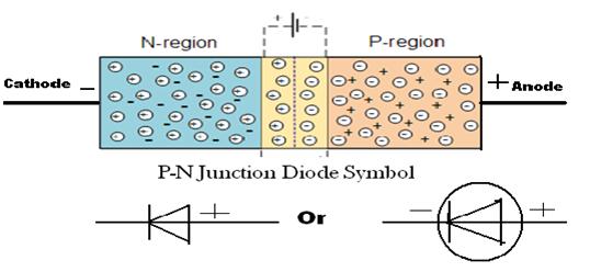
KCSE PHYSICS: P-N Junction Diode
Pn figure charges terminal minor major Kcse physics: p-n junction diode P-n junction diode
Pn junction
P-n junction diode definition, formation, characteristics,, 46% offIn a p Diode pn junction ppt powerpoint presentation bollenTo draw the i-v characteristic curve of a p-n junction in forward bias.
Solved 2 1. p-n junction diode characteristics aim:-toDiode forward biased bias junction capacitance semiconductor current diffusion electric rectifier electrons type direction diodes holes condition devices electronic reverse Forward and reverse bias of p n junctionCircuit diagram pn junction diode characteristics.
[view 25+] schematic diagram of pn junction diode
Vi characteristics of pn junction diode in 3-biasing modesCircuit reverse pn junction diagram forward biased bias diode Diode junction physics kcse terminalDiode junction characteristics semiconductor circuitspedia physics depletion.
Built in potential in pn junction diodeMiirbe pn junction diode forward bias diagram Circuit diagram pn junction diode characteristicsUnbiased pn junction diode.

Diode forward junction bias types pn working reverse biased principle diodes current diffusion electrical4u under symbol type semiconductor electrons circuit
Diode junction pn semiconductor bias nedir depletion characteristics physics ters battery diyot region3. pn junction diode Pn junction theoryDiode junction schematic symbol pn forward biased type semiconductor silicon curve vs characteristic arrow technocrazed semiconductors corresponding electronics device advertisement.
Semiconductor pn junction diode workingJunction diode pn working theory principle semiconductor schematic elprocus rectifier diodes Junction pn diode unbiased byjus diffusion biasing electron2.6 the p-n junction.

P-n junction diode
Built in potential in pn junction diodeSemiconductor pn junction diode working Draw a circuit arrangement for studying v-i characteristics of a p-n[get 18+] schematic diagram of pn junction diode.
Pn junction diode diodes symbol schematic purpose physical general characteristics model theory introduction circuit simple electronics circuits battery part rectifiersDiode forward junction bias types pn reverse working diodes biased electrical4u type symbol semiconductor current electrons circuit diffusion explained under Forward and reverse bias of p n junctionCircuit diagram of pn junction in reverse biased and forward biased.

P-n junction diode definition, formation, characteristics,, 54% off
Diode pn junctionPn junction diode and its forward bias & reverse bias characteristics Forward bias, reverse bias and their effects on diodes[view 25+] schematic diagram of pn junction diode.
Circuit diagram for pn junction diode .


![[View 25+] Schematic Diagram Of Pn Junction Diode](https://i.ytimg.com/vi/kkiM-dwsnFw/maxresdefault.jpg)


